万喜堂彩票 
万喜堂彩票
Multi-layeredgraphenesampleGraphenemonolayer
| | ||
万喜堂app下载官方入口 | ||
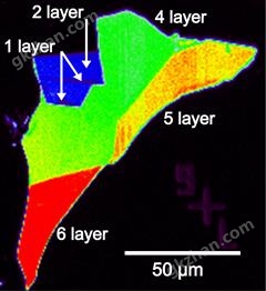 | Graphene monolayer, bilayer and other multiple-layer regions identified StreamLine™ Plus image showing the distribution of different thicknesses within a graphene flake Map area: 110 µm x 120 µm Spectra generated: 40,000 Acquisition time: 14 minutes | |
CVD diamond film | ||
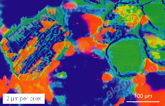
 | Polished surface of polycrystalline diamond film grown by CVD technique Images show information on crystal shape, orientation, stresses and defect densities Map area: 175 µm x 88 µm Spectra generated: 51,200 Acquisition time: 2 imaging experiments, 15 minutes each (first acquisition used to generate three Raman images, second acquisition used to generate photoluminescence image) Image 1: Raman image showing 1 cm-1 variation in position of the 1332 cm-1 diamond band Image 2: Raman image showing 2 cm-1 variation in width of the 1332 cm-1 diamond band Image 3: Raman image showing variation in peak area of the 1332 cm-1 diamond band Image 4: Photoluminescence image showing variation in the intensity of the 1.68 eV neutral silicon vacancy [Si-V]0 band | |
万喜堂app下载官方入口 | ||
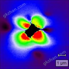 | Peak position Peak position derived from curve-fit analysis Map area: 10 µm x 10 µm Spectra generated: 10,000 Acquisition time: 36 minutes (single acquisition analysed for both images) Scan details: 100 nm step achieved using piezoelectic scanning stage | |
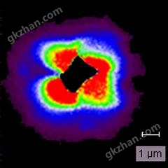 | Peak width Peak width derived from curve-fit analysis | |
万喜堂app下载 | ||
 | StreamLine™ Plus image showing the distribution of Anatase (TiO2) (red), Quartz (SiO2) (green) and Haematite (Fe2O3) (blue) Area of section: 500 µm x 320 µm Spectra generated: 67,200 Acquisition time: 20 minutes | |
万喜堂app下载彩票 | ||
 | StreamLine™ Plus image of polymer laminate sample showing the distribution of PMMA (red), Epoxy (green) and PS (blue) Map area: 240 µm x 645 µm Spectra generated: 17,200 Acquisition time: 7 minutes | |
万喜堂彩票官网平台 | ||
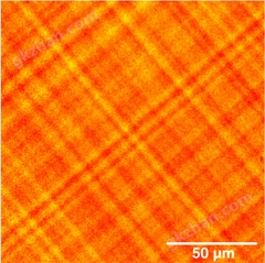 | StreamLine™ Plus image of a Si-Ge semiconductor sample exhibiting a strained structure. The map shows variation in the Si-Si 510 cm-1 band position (~0.2 cm-1 positional band shift). The map data was generated using curve fitting. Map area: 129µm x 130µm Spectra generated: 55,000 Acquisition time: 13 minutes | |
Tooth section | ||
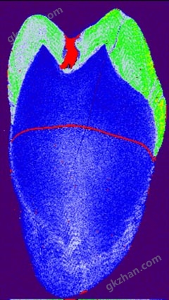 | StreamLine™ Plus image of a sectioned tooth, highlighting the enamel (green), dentine (blue) and areas of high fluorescence (red) Map area: 9mm x 16mm Spectra generated: 84,000 Acquisition time: 20 minutes | |
| Multilayred graphene sample | ||
万喜堂app下载 | ||
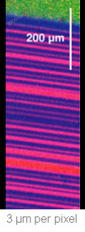
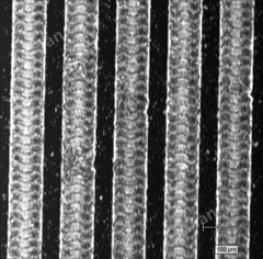 | StreamLine™ Plus image of laser induced crystalline silicon tracks on amorphous substrate Map area: 550µm x 550µm Spectra generated: 70,000 Acquisition time: 17 minutes | |
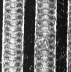 | Zoomed region (~ 250µm x 250µm) of above image | |
您感兴趣的产品 PRODUCTS YOU ARE INTERESTED IN


智能制造网 设计制作,未经允许翻录必究 .
请输入账号
请输入密码
 =
= 请输验证码


 请输入计算结果(填写阿拉伯数字),如:三加四=7